
Field Emission Scanning Electron Microscope Laboratory
The laboratory pouses a TESCAN MIRA3 high performance variable pressure Analytical Electron Microscope with a high resolution of 5.0 nm, along with EDS (Energy Dispersive Spectroscopy), SE (Secondary Electron Detector) and BSE (Back Scattered Electron Detector).
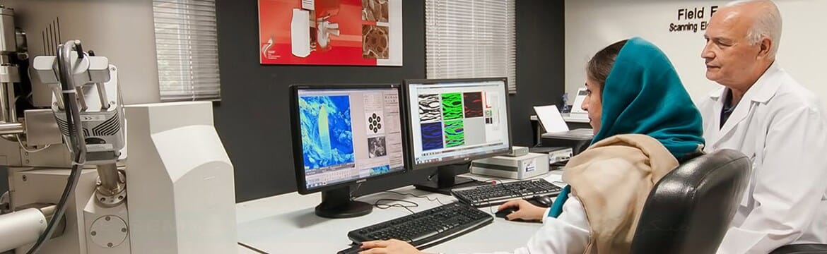
Our state-of-the-art field emission scanning electron Microscope (FESEM) facility with staff who are expert in sample preparation, Imaging and Analysis provides faculty, students and industrial collaborators with the advantages of the latest technology.
The large sample chamber allows for the examination of sample up to 100 mm in diameter and 50 mm in height. High-Resolution images are produced during SEM analysis at magnification from 5X to 500KX.

Common Applications are provided below:
- Materials Science
- Electro-Technical Engineering
- Forensic Investigations
- Research
- Life Sciences

RASF ´s FE-SEM Laboratory Capabilities:
- Providing SEM analysis services for advanced materials, including semiconductors, polymers, nanoparticles and nanotubes, glass and environmental particulate
- High-resolution imaging
- Preparing images at very low accelerating voltage (low kV)
- EDS Analysis –semi-quantitative results
- Point Analysis, Elemental Mapping, Line Scan
- Standard Microscopy Methods to determine the concentration of asbestos
- Sample Coating and Coating thickness Determination
- Surface Morphology and Texture
- Particle size Evaluation
- Fracture Surface Analysis